- 您现在的位置:买卖IC网 > Sheet目录1214 > EVAL-ADE7759EBZ (Analog Devices Inc)BOARD EVALUATION FOR ADE7759
�� ��
��
��ADE7759�
�ALIASING� EFFECTS�
�MAXIMUM�
�OUTPUT�
�IMPEDANCE�
�6k�
�SAMPLING�
�LOAD� =� 10� A�
�REF� IN/OUT�
�IMAGE�
�FREQUENCIES�
�FREQUENCY�
�PTAT�
�60� A�
�1.7k�
�2.42V�
�2.5V�
�12.5k�
�0�
�2�
�447�
�FREQUENCY� –� kHz�
�894�
�12.5k�
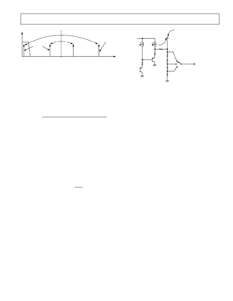
�Figure� 21.� ADC� and� Signal� Processing� in� Channel� 1�
�For� a� di/dt� sensor� such� as� a� Rogowski� coil,� however,� the� sensor�
�has� 20� dB� per� decade� gain.� This� will� neutralize� the� –20� dB� per�
�decade� attenuation� produced� by� this� simple� LPF� and� nullifies�
�12.5k�
�12.5k�
�REFERENCE� INPUT�
�TO� ADC� CHANNEL� 1�
�(RANGE� SELECT)�
�2.42V,� 1.21V,� 0.6V�
�the� antialias� filter.� Therefore,� when� using� a� di/dt� sensor,� mea-�
�sures� should� be� taken� to� offset� the� 20� dB� per� decade� gain� coming�
�from� the� di/dt� sensor� and� produce� sufficient� attenuation� to�
�eliminate� any� aliasing� effect.� One� simple� approach� is� to� cascade�
�two� RC� filters� to� produce� –40� dB� per� decade� attenuation.� The�
�Figure� 22.� ADC� and� Reference� Circuit� Output�
�The� REF� IN/OUT� pin� can� be� overdriven� by� an� external� source,�
�e.g.,� an� external� 2.5� V� reference.� Note� that� the� nominal� refer-�
�ence� value� supplied� to� the� ADCs� is� now� 2.5� V� not� 2.42� V.� This�
�has� the� effect� of� increasing� the� nominal� analog� input� signal�
�transfer� function� for� a� cascaded� filter� is� the� following:�
�range� by� 2.5/2.42�
�100%� =� 3%,� or� from� 0.5� V� to� 0.5165� V.�
�H� (� s� )� =�
�1� +� sR� 1� C� 1� +� sR� 2� C� 2� +� sR� 1� C� 2� +� s� R� 1� C� 1� R� 2� C� 2�
�Code� (� ADC� )� =� 3� .� 0492� �
�� 262� ,� 144�
�1�
�2�
�where� R� 1� C� 1� represents� the� RC� used� in� the� first� stage� of� the�
�cascade� and� R� 2� C� 2� in� that� of� the� second� stage.� The� s� 2� term� in� the�
�transfer� function� produces� a� –40� dB/decade� attenuation.� Note�
�that� to� minimize� the� measurement� error,� especially� at� low� power�
�factor,� it� is� important� to� match� the� phase� angle� between� the�
�voltage� and� the� current� channel.� The� small� phase� mismatch� in�
�the� external� antialias� filter� can� be� corrected� using� the� phase� calibra-�
�tion� register� (PHCAL[7:0])—see� Phase� Compensation� section� .�
�ADC� Transfer� Function�
�Below� is� an� expression� which� relates� the� output� of� the� LPF� in�
�the� sigma-delta� ADC� to� the� analog� input� signal� level.� Both� ADCs�
�in� the� ADE7759� are� designed� to� produce� the� same� output� code�
�for� the� same� input� signal� level.�
�V� IN�
�V� REF�
�Therefore,� with� a� full-scale� signal� on� the� input� of� 0.5� V� and� an�
�internal� reference� of� 2.42� V,� the� ADC� output� code� is� nominally�
�165,151� or� 2851Fh.� The� maximum� code� from� the� ADC� is�
�±� 262,144,� which� is� equivalent� to� an� input� signal� level� of� ±� 0.794� V.�
�However,� for� specified� performance� it� is� not� recommended� that� the�
�full-scale� input� signal� level� of� 0.5� V� be� exceeded.�
�Reference� Circuit�
�Shown� in� Figure� 22� is� a� simplified� version� of� the� reference� out-�
�put� circuitry.� The� nominal� reference� voltage� at� the� REF� IN/OUT�
�pin� is� 2.42� V.� This� is� the� reference� voltage� used� for� the� ADCs� in�
�the� ADE7759.� However,� Channel� 1� has� three� input� range� selec-�
�tions,� which� are� selected� by� dividing� down� the� reference� value�
�used� for� the� ADC� in� Channel� 1.� The� reference� value� used� for�
�Channel� 1� is� divided� down� to� 1/2� and� 1/4� of� the� nominal� value�
�by� using� an� internal� resistor� divider,� as� shown� in� Figure� 22.�
�REV.� A�
�The� internal� voltage� reference� on� the� ADE7759� has� a� tempera-�
�ture� drift� associated� with� it—see� ADE7759� Specifications� section�
�for� the� temperature� coefficient� specification� (in� ppm� °� C).� The�
�value� of� the� temperature� drift� varies� slightly� from� part� to� part.�
�Since� the� reference� is� used� for� the� ADCs� in� both� Channel� 1� and� 2,�
�any� x%� drift� in� the� reference� will� result� in� 2x%� deviation� of� the�
�meter� reading.� The� reference� drift� resulting� from� temperature�
�changes� is� usually� very� small,� and� it� is� typically� much� smaller�
�than� the� drift� of� other� components� on� a� meter.� However,� if�
�guaranteed� temperature� performance� is� needed,� one� needs� to�
�use� an� external� voltage� reference.� Alternatively,� the� meter� can� be�
�calibrated� at� multiple� temperatures.� Real-time� compensation�
�can� be� achieved� easily� using� the� on-chip� temperature� sensor.�
�CHANNEL� 1� ADC�
�Figure� 23� shows� the� ADC� and� signal� processing� chain� for� Chan-�
�nel� 1.� In� waveform� sampling� mode,� the� ADC� outputs� a� signed�
�twos� complement� 20-bit� dataword� at� a� maximum� of� 27.9� kSPS�
�(CLKIN/128).� The� output� of� the� ADC� can� be� scaled� by� ±� 50%�
�to� perform� an� overall� power� calibration� or� to� calibrate� the� ADC�
�output.� While� the� ADC� outputs� a� 20-bit� twos� complement�
�value,� the� maximum� full-scale� positive� value� from� the� ADC� is�
�limited� to� 40,000h� (+262,144� decimal).� The� maximum� full-�
�scale� negative� value� is� limited� to� C0000h� (–262,144� decimal).� If�
�the� analog� inputs� are� overranged,� the� ADC� output� code� will�
�clamp� at� these� values.� With� the� specified� full-scale� analog� input�
�signal� of� 0.5� V� (or� 0.25� V� or� 0.125� V—see� Analog� Inputs� sec-�
�tion),� the� ADC� will� produce� an� output� code� that� is� approximately�
�63%� of� its� full-scale� value.� This� is� illustrated� in� Figure� 23.� The�
�diagram� in� Figure� 23� shows� a� full-scale� voltage� signal� being�
�applied� to� the� differential� inputs� V1P� and� V1N.� The� ADC�
�output� swings� between� D7AE1h� (–165,151)� and� 2851Fh�
�(+165,151).� This� is� approximately� 63%� of� the� full-scale� value�
�40,000h� (262,144).� Overranging� the� analog� inputs� with� more�
�than� 0.5� V� differential� (0.25� V� or� 0.125� V,� depending� on�
�Channel� 1� full-scale� selection)� will� cause� the� ADC� output� to�
�increase� towards� its� full-scale� value.� However,� for� specified�
�operation,� the� differential� signal� on� the� analog� inputs� should�
�not� exceed� the� recommended� value� of� 0.5� V.�
�–17� –�
�发布紧急采购,3分钟左右您将得到回复。
相关PDF资料
EVAL-ADE7762EBZ
BOARD EVALUATION FOR ADE7762
EVAL-ADE7763ZEB
BOARD EVALUATION FOR ADE7763
EVAL-ADE7816EBZ
BOARD EVALUATION FOR ADE7816
EVAL-ADE7878EBZ
BOARD EVAL FOR ADE7878
EVAL-ADE7880EBZ
BOARD EVAL FOR ADE7880
EVAL-ADE7953EBZ
BOARD EVAL FOR ADE7953
EVAL-ADF4002EBZ1
BOARD EVAL FOR ADF4002
EVAL-ADG788EBZ
BOARD EVALUATION FOR ADG788
相关代理商/技术参数
EVAL-ADE7762EBZ
功能描述:BOARD EVALUATION FOR ADE7762 RoHS:是 类别:编程器,开发系统 >> 评估演示板和套件 系列:- 标准包装:1 系列:- 主要目的:电信,线路接口单元(LIU) 嵌入式:- 已用 IC / 零件:IDT82V2081 主要属性:T1/J1/E1 LIU 次要属性:- 已供物品:板,电源,线缆,CD 其它名称:82EBV2081
EVAL-ADE7763EB
制造商:Analog Devices 功能描述:EVALUATION BOARD DOCUMENTATION ADE7763 ENERGY METERING IC
EVAL-ADE7763ZEB
功能描述:BOARD EVALUATION FOR ADE7763 RoHS:是 类别:编程器,开发系统 >> 评估演示板和套件 系列:- 标准包装:1 系列:PSoC® 主要目的:电源管理,热管理 嵌入式:- 已用 IC / 零件:- 主要属性:- 次要属性:- 已供物品:板,CD,电源
EVAL-ADE7816EBZ
功能描述:BOARD EVALUATION FOR ADE7816 RoHS:是 类别:编程器,开发系统 >> 评估演示板和套件 系列:- 标准包装:1 系列:PSoC® 主要目的:电源管理,热管理 嵌入式:- 已用 IC / 零件:- 主要属性:- 次要属性:- 已供物品:板,CD,电源
EVAL-ADE7854EBZ
制造商:Analog Devices 功能描述:EVALUATION BOARDS - Boxed Product (Development Kits)
EVAL-ADE7858EBZ
制造商:AD 制造商全称:Analog Devices 功能描述:Poly Phase Multifunction Energy Metering IC with per Phase Active and Reactive Powers
EVAL-ADE7878EBZ
功能描述:BOARD EVAL FOR ADE7878 RoHS:是 类别:编程器,开发系统 >> 评估演示板和套件 系列:- 标准包装:1 系列:PCI Express® (PCIe) 主要目的:接口,收发器,PCI Express 嵌入式:- 已用 IC / 零件:DS80PCI800 主要属性:- 次要属性:- 已供物品:板
EVAL-ADE7880EBZ
功能描述:BOARD EVAL FOR ADE7880 RoHS:是 类别:编程器,开发系统 >> 评估演示板和套件 系列:* 产品培训模块:Obsolescence Mitigation Program 标准包装:1 系列:- 主要目的:电源管理,电池充电器 嵌入式:否 已用 IC / 零件:MAX8903A 主要属性:1 芯锂离子电池 次要属性:状态 LED 已供物品:板